Gain a deeper understanding of scanning array radar signal processing
Active electronically scanned array (AESA) radar technology is a core component of modern advanced weapon systems, especially playing an important role in airborne combat platforms. In the future, the development of AESA architecture will not be limited to its initial military use, but will also expand to multiple fields such as geophysical measurements, automotive assisted driving systems, autonomous vehicles, industrial automation, and even augmented reality – all of which require processing large amounts of sensor data and integrating it into decision models. With the continuous popularization of AESA technology, its application scope will exceed the professional radar signal processing field and penetrate into a wider range of scenarios. In these new application environments, AESA design will follow the common embedded system development process, which is centered around the central processing unit (CPU) and software, using C language as the foundation and decoupled from hardware. In this article, we will explore the architecture evolution of AESA radar from the perspectives of senior radar signal processing experts and traditional embedded system designers.
The role of a typical system
The main difference between scanning array radar and traditional mobile disk radar lies in the design of the antenna. Scanning array radar does not use the common continuous rotating parabolic antenna, but mostly uses a fixed planar antenna. In this array, it is not just one unit focused on the reflector, but is composed of hundreds to thousands of units, each with its own transceiver module. The electronic circuit in the system is responsible for processing the amplitude and phase of each unit signal to form the directional pattern of the radar beam, and focusing it to define the directional pattern of the entire antenna.
This method reduces the dependence on mechanical moving parts, allowing the radar to achieve functions that traditional antennas cannot achieve, such as instantly changing the direction of the beam and performing transmission and reception operations in multiple directions, or dividing the array into multiple sub arrays to perform different tasks, such as terrain detection while tracking targets. To achieve these functions, it is only necessary to add specific signals in the transmitter and separate the signals in each receiver. This method is commonly referred to as beamforming or spatial multiplexing technology.
A complete radar system starts from the CPU cluster, where the signal is transmitted to the antenna and then the echo signal is received (as shown in Figure 1). In the early stages of signal processing, a software controlled waveform generator generates the chirp signal (a signal whose frequency varies linearly with time) that the system needs to send. Depending on the specific application, noise reduction, Doppler processing, and consideration of stealth technology may be necessary, all of which can affect the quality and effectiveness of the signal.
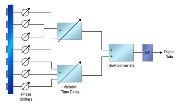
Figure 1. A very simplified AESA system architecture diagram.
The signal generated by the waveform generator will be sent to the beamforming network, where the signal is assigned to each transmission channel. At this stage, the digital multiplexer applies amplitude weighting on each channel to achieve spatial filtering and shape the waveform. This process can also be postponed to subsequent steps. In many design schemes, the signal from each channel is then passed through a digital to analog converter (DAC) before entering analog intermediate frequency (IF) and radio frequency (RF) upconverters. After RF up conversion, the signal will be sent to an independent transmission module where phase shift or delay is added and amplitude is adjusted (if not previously done in the baseband), and finally filtered and amplified.
During the receiving process, the signal is transmitted through the opposite path. At each antenna unit, the signal first passes through a limiter and bandpass filter to protect the low-noise amplifier. The amplified signal drives the RF down converter, which may include analog amplification and phase adjustment functions. The signal is transmitted from the intermediate frequency (IF) level to the baseband, and the signal of each antenna unit is sent to its respective analog-to-digital converter (ADC). Afterwards, the beamforming module recombines the antenna signals into one or more complex data sample streams, each representing a signal from a certain receiving beam. These signal streams are then passed through high load digital signal processing (DSP) circuits to further process the data, perform Doppler processing, and attempt to extract useful signals from background noise.
When to perform data conversion
In many traditional designs, most signal processing work is done through analog methods. However, with the advancement of digital technology, especially the improvement of data converter speed, reduction of power consumption, and decrease in cost, data converters are gradually approaching antenna units. Colman Cheung, an application expert at Altera, proposed an idealized system concept that directly drives antenna units from a digital to analog converter (DAC). However, as of 2013, such designs were not yet fully mature in technology, especially in the field of trans GHz RF.
At present, data converters can be placed in the intermediate frequency (IF) layer for IF frequency conversion, and all baseband processing work is fully digitized (as shown in Figure 2). In the baseband beamforming network, the required time delay for generating interference patterns between antenna units can be generated digitally, without the need for each antenna unit to be equipped with an analog phase shifter or delay line. This approach allows digital signal processing (DSP) designers to decompose the transmission and reception paths into independent functional modules, such as multipliers, filters, FIFO (first in first out queue) for delay, and adders, and model and simulate these modules in tools such as MATLAB, thereby utilizing existing libraries to implement them.
For computationally intensive tasks, they can be deployed on specially customized ASICs (Application Specific Integrated Circuits), FPGAs (Field Programmable Gate Arrays), or GPUs (Graphics Processing Units), while simpler operations can be completed by writing code that runs on DSP chips or accelerators. This flexibility allows system design to be optimized based on performance and cost requirements.
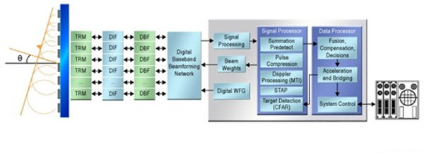
Figure 2. Place the data converter at the end of the IF stage.
In signal processing, it is particularly important to pay attention to the processing of the receiving chain after the signal is output from the beamforming network. This is because the storage and computing requirements at this stage are extremely large, and the dynamic range involved is very wide – from interfering with the input signal of the transmitter to the limit of the search and detection range. This requires the use of high-precision floating-point hardware and a system with powerful processing capabilities.
In the final stage of the receiving chain, targeted modifications and implementations were made to the receiving chain. The main task of the receiving chain is to extract signals from noise, especially those that may contain actual target information in the environment, through processing stages such as filtering, beam focusing, and pulse compression. Once the signal is extracted, the focus shifts from the signal itself to the target it represents, and the focus of the task also changes accordingly.
From signal to target
Pulse compression marks the starting point of this abstract processing process. Pulse compressors typically use autocorrelation techniques in the time or frequency domain to identify waveforms that may contain transmit chirps. Then, it represents these waveforms as pulse targets – data packets containing arrival time, frequency, phase, and other relevant information. From this point on, the receiving chain processes these data packets, not the original received signals.
The next step is usually to perform Doppler processing. Firstly, the pulses are organized into a grid array (as shown in Figure 3). In this array, each column contains pulses returned from a specific emission chirp. There are many columns in the array, depending on the maximum delay time that the system can tolerate. The rows in the array represent the return switching time: the farther away from the x-axis of the array, the greater the delay between the arrival time of the transmitted chirp and the received pulse. Therefore, these delay grids also represent the distance to the target corresponding to the reflected pulse.
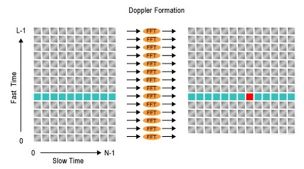
Figure 3. Doppler processing grid.
After placing a series of chirped pulses into the correct grid, the Doppler processing program will horizontally move the data, observe the changes in pulses returned from a single target over time, and extract information about relative velocity and target direction. This processing method requires a large circular buffer, which must be able to accommodate all grid data regardless of how many grids the Doppler algorithm can process at once.
In more advanced systems, a third dimension has been added to the array. By dividing the antenna array into sub arrays, the system can simultaneously transmit multiple beams and use receivers configured with the same or multiple beam antenna patterns to listen. Alternatively, the system can scan the beam using beamforming or synthetic aperture techniques. When loading compressed pulses, the system constructs a three-dimensional grid array: one axis represents the emitted pulses, the second axis represents the return delay, and the third axis represents the direction of the beam (as shown in Figure 4). In this way, for each pulse, we have a two-dimensional or three-dimensional grid array, representing both distance and direction – that is, representing physical space. This memory layout is the foundation of Space Time Adaptive Processing (STAP).
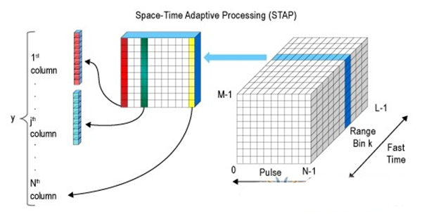
Figure 4. Multidimensional grid is used to establish the matrix for STAP.
This term can be explained as “space-time”, where the dataset unifies the position of the target in three-dimensional space and includes chirp times related to the target. The reason why it is called “adaptive” is because algorithms can obtain the effect of adaptive filtering from data.
Conceptually, and in practical operation, the process of building an adaptive filter involves matrix inversion: finding a matrix to multiply with data to reveal the results hidden in noise. According to Michael Parker, Senior Technology Marketing Manager at Altera, the information used to infer hidden directional patterns may come from clues discovered during Doppler processing, data collected by other sensors, or intelligent data. The algorithm running on the CPU inserts the assumed directional diagram into the matrix equation to solve for the filtering function that can generate the expected data.
Obviously, at this point, the computational load is enormous. The dynamic range required for the inverse conversion method requires the use of floating-point operations. For an actual medium-sized system in a combat environment, real-time processing of this data is necessary, and Parker estimates that the STAP load will reach several TFLOPS (trillions of floating-point operations per second). In systems that use low resolution and narrow dynamic range, such as simple car assisted driving systems or synthetic aperture imaging systems, real-time requirements are lower, resulting in a significant reduction in computational load.
The information processed from STAP will be passed to a general-purpose CPU for more complex but computationally efficient operations. The software will attempt to classify targets, build environmental models, assess threats or notify operators, and even take emergency measures directly. At this stage, we not only process signals in the signal processing domain, but also enter the field of artificial intelligence.
Two architectures
From the perspective of an experienced radar system designer, our understanding of AESA combat radar is quite superficial. This perspective views the network as a relatively static DSP chain, with all parts connected to the STA module, which is essentially a matrix arithmetic unit controlled by software. Furthermore, from the perspective of DSP experts, this is a set of CPU cores.
By contrast, designers of automotive or robotic systems may approach this issue from a completely different perspective. For embedded system designers, the entire system is more like a large collection of software, containing highly specialized I/O devices and tasks that require acceleration. For professionals familiar with radar signal processing, considering the ratio of signal processing to general hardware, they may be puzzled by this software centric approach. It is evident that the data rate, flexibility, and dynamic range of airborne multifunctional radar require the use of dedicated DSP pipelines and a large amount of local buffering to achieve real-time processing. But for different applications with fewer antenna units, simple environments, shorter distances, and lower resolutions, the CPU centric perspective brings some interesting issues.
Rice University professor Gene Frantz proposed two key questions: first, defining the real I/O environment; The second is to choose a suitable CPU. Frantz pointed out that “rarely only one CPU, more commonly heterogeneous multiprocessor systems.” He suggested that this design approach should not start with DSP functions in MATLAB, but with the entire system described in C language. Then, CPU centric designers do not define the hardware boundaries between DSP and CPU domains, but rather “continuously optimize and accelerate C code
The actual results may differ greatly from the DSP centered approach. For example, the CPU centric approach initially assumes that all tasks are executed on a general-purpose CPU. If the speed is not fast enough, this method will shift to multi CPU systems, sharing a layered unified memory. Only when multi-core processing is insufficient to complete the task, will we turn to optimized hardware accelerators.
Similarly, CPU centric design starts with assuming a unified memory. It allocates continuous cache for each processor and local working memory for accelerators. It does not assume any hardware pipeline at the beginning, nor does it map tasks to hardware resources.
In the most demanding applications, the same system design may adopt two architectural methods simultaneously. The strict bandwidth and computing requirements of almost every task prompt the use of dedicated hardware pipelines and memory instantiation. In order to significantly reduce power consumption, higher precision digital methods may be required, which makes hardware sharing between tasks more complex.
Accuracy is an aspect emphasized by Frantz. He pointed out that “reducing the number of significant bits by half can improve performance by an order of magnitude.” In order to reduce power consumption, compromises or partial compromises can be made in this regard.
Frantz also mentioned the issue of analog/digital boundaries. He said, “We need to re-examine analog signal processing. Thirty years ago, we started telling system designers that as long as data conversion is done well, the rest can be solved using digital methods. But in the case of 8-bit resolution, analog and digital methods are basically equivalent. Is analog method better? It depends on what ‘better’ means in your system
Narrowband systems such as synthetic aperture radar used in geophysical mapping or automatic land vehicle systems will adopt a completely different architecture from combat radar. It can use analog filters, up/down converters, and beamforming functions to complete the subsequent processing work of broadband storage systems, and use multiple heterogeneous processors with floating-point accelerators and dynamic load balancing functions (as shown in Figure 5).
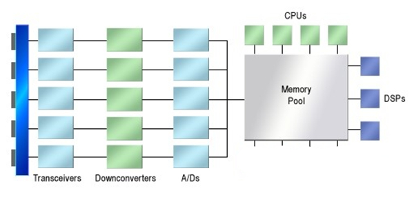
Figure 5. An ideal low performance AESA system.
Visualizing signal processing tasks and completing them in software provides system designers with new runtime options, such as dynamically allocating processing resources between different tasks, turning off unnecessary processors, adjusting algorithms early based on data patterns, or running multiple algorithms simultaneously to determine which one produces the best results.
The AESA radar system not only provides a rich environment for exploring implementation strategies, but also provides a means for studying how to handle systems with large amounts of signals. These active arrays are not only used in the military field, but also have a wide range of applications in many other designs. Therefore, thinking should not be limited to traditional embedded design concepts. For fields that also require processing large amounts of signals, new ways of thinking should be adopted, including applications such as signal intelligence and network security. These are all areas worth paying attention to.
